
Author Affiliations
Abstract
1 State Key Laboratory on Integrated Optoelectronics, College of Electronic Science and Engineering, Jilin University, Changchun 130012, China
2 Peng Cheng Laboratory, Shenzhen 518000, China
Lidar based on the optical phased array (OPA) and frequency-modulated continuous wave (FMCW) technology stands out in automotive applications due to its all-solid-state design, high reliability, and remarkable resistance to interference. However, while FMCW coherent detection enhances the interference resistance capabilities, it concurrently results in a significant increase in depth computation, becoming a primary constraint for improving point cloud density in such perception systems. To address this challenge, this study introduces a lidar solution leveraging the flexible scanning characteristics of OPA. The proposed system categorizes target types within the scene based on RGB images. Subsequently, it performs scans with varying angular resolutions depending on the importance of the targets. Experimental results demonstrate that, compared to traditional scanning methods, the target-adaptive method based on semantic segmentation reduces the number of points to about one-quarter while maintaining the resolution of the primary target area. Conversely, with a similar number of points, the proposed approach increases the point cloud density of the primary target area by about four times.
Photonics Research
2024, 12(5): 904
1 中国科学院 长春光学精密机械与物理研究所 发光学及应用国家重点实验室, 吉林长春30033
2 中国科学院大学 材料与光电研究中心,北京100049
3 吉林大学 电子科学与工程学院,吉林长春10012
4 鹏城实验室,广东深圳518055
在调频连续波激光雷达中,用于中频信号采集的模拟-数字采集模块是其关键组件,信噪比、信纳比、无杂散动态范围等参数是衡量该数据采集信号链交流特性的重要指标,直接决定着调频连续波激光雷达的探测范围和测距精度等性能。设计了用于调频连续波激光雷达的中频信号采集模块,获得49.13 dB的信噪比和48.90 dB的信纳比;然后研究了其噪声特性,获得系统的主要噪声来源为采样时钟的相位噪声,并且通过引入数字滤波器将信噪比和信纳比分别提升11.38 dB和11.32 dB,理论上激光雷达的探测范围提高3.7倍。可通过采用专业时钟芯片降低噪声,经计算可将信噪比提高8.65 dB;最后,搭建了光学相控阵调频连续波激光雷达系统,验证了数据采样模块的有效性,完成了40 m距离的探测,最大测量误差为7.7 cm,最大探测范围为133.67 m。
激光雷达 调频连续波 ADC信号链 噪声分析 lidar frequency-modulated continuous-wave ADC signal chain noise analysis 
Author Affiliations
Abstract
1 State Key Laboratory of Integrated Optoelectronics, College of Electronic Science and Engineering, Jilin University, Changchun 130012, China
2 Advance Micro Foundry Pte Ltd, Singapore 117685, Singapore
3 Peng Cheng Laboratory, Shenzhen 518000, China
Germanium-on-silicon (Ge-on-Si) avalanche photodiodes (APDs) are widely used in near-infrared detection, laser ranging, free space communication, quantum communication, and other fields. However, the existence of lattice defects at the Ge/Si interface causes a high dark current in the Ge-on-Si APD, degrading the device sensitivity and also increasing energy consumption in integrated circuits. In this work, we propose a novel surface illuminated Ge-on-Si APD architecture with three terminals. Besides two electrodes on Si substrates, a third electrode is designed for Ge to regulate the control current and bandwidth, achieving multiple outputs of a single device and reducing the dark current of the device. When the voltage on Ge is , the proposed device achieves a dark current of 100 nA, responsivity of 9.97 A/W at input laser power at 1550 nm, and optimal bandwidth of 142 MHz. The low dark current and improved responsivity can meet the requirements of autonomous driving and other applications demanding weak light detection.
Photonics Research
2022, 10(8): 1956

Author Affiliations
Abstract
1 State Key Laboratory of Integrated Optoelectronics, College of Electronic Science and Engineering, Jilin University, Changchun 130012, China
2 CAS Key Laboratory of Quantum Information, University of Science and Technology of China, Hefei 230026, China
3 CAS Center for Excellence in Quantum Information and Quantum Physics, University of Science and Technology of China, Hefei 230026, China
4 Advanced Micro Foundry Pte Ltd., Singapore 117685, Singapore
5 Peng Cheng Laboratory, Shenzhen 518000, China
To optimize the dark current characteristic and detection efficiency of the 1550 nm weak light signal at room temperature, this work proposes a Ge-on-Si avalanche photodiode (APD) in Geiger mode, which could operate at 300 K. This lateral separate absorption charge multiplication APD shows a low breakdown voltage (Vbr) in Geiger mode of and low dark current of 0.096 nA at unity gain voltage (VGain=1 = -7.03 V). Combined with an RF amplifier module and counter, the detection system demonstrates a low dark count rate (DCR) of per second and high detection efficiency of 7.8% for 1550 nm weak coherent pulse detection at 300 K. The APD reported in this work weakens the dependence of the weak optical signal recognition on the low environment temperature and makes single-chip integration of the single-photon level detection system possible.
avalanche photodiode optical detection optical interconnection Chinese Optics Letters
2022, 20(6): 062501

Author Affiliations
Abstract
1 State Key Laboratory on Integrated Optoelectronics, College of Electronic Science and Engineering, Jilin University, Changchun 130012, China
2 Peng Cheng Laboratory, Shenzhen 518000, China
3 Advance Micro Foundry Pte. Ltd., Singapore 117685, Singapore
Optical phased array (OPA) technology is considered a promising solution for solid-state beam steering to supersede the traditional mechanical beam steering. As a key component of the LIDAR system for long-range detection, OPAs featuring a wide steering angle and high resolution without beam aliasing are highly desired. However, a wide steering range requires a waveguide pitch less than half of the wavelength, which is easily subjected to cross talk. Besides, high resolution requires a large aperture, and it is normally achieved by a high count number of waveguides, which complicates the control system. To solve the mentioned issues, we design two high-performance 128-channel OPAs fabricated on a multilayered SiN-on-SOI platform. Attributed to the nonuniform antenna pitch, only 128 waveguides are used to achieve a 4 mm wide aperture. Besides, by virtue of innovative dual-level silicon nitride () waveguide grating antennas, the fishbone antenna OPA achieves a field of view (FOV) with divergence of , and the chain antenna OPA realizes a FOV with divergence of . To our best knowledge, 140° is the widest lateral steering range in two-dimensional OPA, and 0.029° is the smallest longitudinal divergence. Finally, we embed the OPA into a frequency-modulated continuous-wave system to achieve 100 m distance measurement. The reflected signal from 100 m distance is well detected with 26 dBm input transmitter power, which proves that OPA serves as a promising candidate for transceiving optical signal in a LIDAR system.
Photonics Research
2021, 9(12): 12002511
Author Affiliations
Abstract
1 State Key Laboratory on Integrated Opto-Electronics, College of Electronic Science and Engineering, Jilin University, Changchun 130012, China
2 Key Laboratory of Quantum Information, University of Science and Technology of China, Hefei 230026, China
The continuous-time quantum walk (CTQW) is the quantum analogue of the continuous-time classical walk and is widely used in universal quantum computations. Here, taking the advantages of the waveguide arrays, we implement large-scale CTQWs on chips. We couple the single-photon source into the middle port of the waveguide arrays and measure the emergent photon number distributions by utilizing the fiber coupling platform. Subsequently, we simulate the photon number distributions of the waveguide arrays by considering the boundary conditions. The boundary conditions are quite necessary in solving the problems of quantum mazes.
270.5570 Quantum detectors 270.0270 Quantum optics Chinese Optics Letters
2019, 17(5): 052701
吉林大学电子科学与工程学院集成光电子学国家重点联合实验室, 吉林 长春 130012
光控相控阵(OPA)不需要机械转动即可实现光束在空间内的扫描,在激光测距以及自由空间光通信等领域具有广阔的应用前景。硅基光电子集成技术可在芯片上实现光电子器件的大规模集成,并与互补金属氧化物半导体(CMOS)集成电路工艺技术完全兼容,以其制作的光控相控阵具有扫描速度快、体积小、成本低、功耗低等特点。目前报道的利用硅基光电子集成技术制作的相控阵,最大的横向扫描范围为80°,最大的纵向扫描范围为36°。简述了硅基光电子集成相控阵的扫描原理,并对国内外最新的研究成果进行了分析总结,最后指出此种技术实用化过程中亟待解决的关键问题,并提出了一些可以提升性能的方案。
光电子学 光控相控阵 集成光电子器件 光束扫描 激光雷达 激光与光电子学进展
2018, 55(5): 050001
Author Affiliations
Abstract
1 Institute of Microelectronics, Agency for Science, Technology and Research (A*STAR), 2 Fusionopolis Way, #08-02, Innovis, Singapore 138634, Singapore
2 Department of Electrical & Computer Engineering, National University of Singapore, 4 Engineering Drive 3, Singapore 117583, Singapore
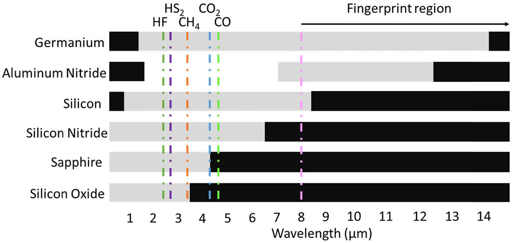
Silicon photonic integrated circuits for telecommunication and data centers have been well studied in the past decade, and now most related efforts have been progressing toward commercialization. Scaling up the silicon-on-insulator (SOI)-based device dimensions in order to extend the operation wavelength to the short mid-infrared (MIR) range (2–4 μm) is attracting research interest, owing to the host of potential applications in lab-on-chip sensors, free space communications, and much more. Other material systems and technology platforms, including silicon-on-silicon nitride, germanium-on-silicon, germanium-on-SOI, germanium-on-silicon nitride, sapphire-on-silicon, SiGe alloy-on-silicon, and aluminum nitride-on-insulator are explored as well in order to realize low-loss waveguide devices for different MIR wavelengths. In this paper, we will comprehensively review silicon photonics for MIR applications, with regard to the state-of-the-art achievements from various device demonstrations in different material platforms by various groups. We will then introduce in detail of our institute’s research and development efforts on the MIR photonic platforms as one case study. Meanwhile, we will discuss the integration schemes along with remaining challenges in devices (e.g., light source) and integration. A few application-oriented examples will be examined to illustrate the issues needing a critical solution toward the final production path (e.g., gas sensors). Finally, we will provide our assessment of the outlook of potential future research topics and engineering challenges along with opportunities.
(130.0130) Integrated optics (130.3120) Integrated optics devices (130.6622) Subsystem integration and techniques. Photonics Research
2017, 5(5): 05000417
吉林大学 电子科学与工程学院集成光电子学国家重点联合实验室吉林大学实验区,吉林 长春 130012
高功率阵列半导体激光器已得到广泛应用,对其质量和可靠性进行无损检测很有必要。在导数测试技术中,参数h是电导数曲线阈值处的下沉高度,参数Q是二阶光导数曲线阈值处的峰的高宽比。对导数测试参数h,Q与阵列激光器的单元器件的质量和均匀性进行了研究。基于其等效电路在一定条件下,计算了阵列激光器的均匀性对h的影响。并对实际阵列器件进行了导数测试。理论和实验结果对比表明,h,Q等参数是组成阵列的各管芯的均匀性的灵敏参数。
激光器 阵列半导体激光器 可靠性检测 导数技术


